ECpE Department receives major external research awards

During the months of July through September 2016, Iowa State University’s Department of Electrical and Computer Engineering received many external research awards from the Department of Energy (DOE), the National Science Foundation (NSF) and other groups.

Coover in the FallMajor grants from the DOE include an award of $1,162,477 for a project entitled “Autonomous Tools for Attack Surface Reduction,” with Manimaran Govindarasu as Principal Investigator (PI) and Venkataramana Ajjarap and Doug Jacobson as Co-Principal Investigators (Co-PI). The total anticipated amount of the award is $2,981,103. The DOE also awarded $1,318,903 for a project called “Novel Light Extraction and Utilization, Organic LED (OLED) Core Technology Research: Enhanced Light Extraction from Low Cost White OLEDs (WOLEDs) Fabricated on Novel Patterned Substrates,” with Ruth Shinar as PI and Rana Biswas and Joseph Shinar as Co-PIs.

A variety of projects received grants from the NSF, with one highlight being $4,054,476 for the project “WI-ECSEL Scholarship Program (Women in Electrical, Computer, and Software Engineering as Leaders,” with Joseph Zambreno as PI and Doug Jacobson, Phillip Harrison Jones, Lisa Larson, Mani Mina, Sarah Rajala, Sarah Rodriguez, Diane Rover and Mack Shelley as Co-PIs.

For more information on grants received during the months of July through September, visit this link: https://www.ece.iastate.edu/external-research-awards-july-september-2016/.
Best Student Paper Award at Photonics West 2016

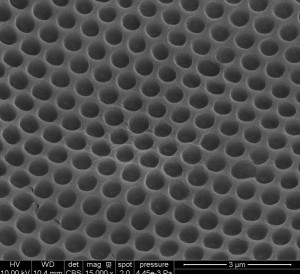
SEM image of the PDMS patterns. The nano-cones are formed from the negative of replication of nano-pits on the PC master pattern.

This year’s Best Student Paper Award in the Microfluidics, BioMEMS, and Medical Microsystems section of  SPIE Photonics West (BIOS) was presented to Iowa State graduate students and faculty for their presentation, “Transfer molding processes for nanoscale patterning of poly-L-lactic acid (PLLA) films.”

This is a collaborative project being performed in ECpE and the Microelectronics Research Center (MRC) by Rabin Dhakal, Akshit Peer, Rana Biswas and Jaeyoun Kim. The team’s presentation was selected out of 48 total oral and poster presentations in the conference held Feb. 13-18 in San Francisco.

The goal of the team’s project is to find novel bio-medical applications of periodically patterned polymeric nano-structures. The group investigated how the surfaces of cardiac stents made of bio-degradable poly-L-lactic acid (PLLA) can be engineered to control and slow down the release of certain drugs, such as anti-coagulant, coated on them.  They developed a soft lithographic method for imprinting intricate periodic nano-patterns onto these stents and demonstrated that large area arrays of nano-cones or nano-cups with pitch of ~700 nm could be effectively nano-imprinted onto the bio-degradable polymer films. The team is currently studying the release dynamics of drugs coated on these patterned surfaces of PLLA- an area that has much promise for applications to treatment of cardiac disease.

Faculty members, Biswas and Kim said they were grateful for the opportunity and glad to have been recognized for their work. 
For more information about the SPIE conference and awards, click here.

Optical transmission technique published

ECpE professor, Rana Biswas, and his PhD student were featured in Optics and Photonics News and in Nanoscale last week.

Research by Rana Biswas, ECpE professor, and Akshit Peer, ECpE PhD student, was featured in Optics and Photonics News and in Nanoscale last week.

Bisa and Peer’s work demonstrates a technique for achieving an optical transmission, with modeled electric-field enhancements as high as a hundredfold, using a continuous film of gold on a corrugated, “nanocupped” substrate. The technique only requires soft-lithography fabrication and can create large-area films.

According to Peer, the ability both to inexpensively create these large-area films and to straightforwardly measure their optical properties makes them a great platform for experiments and applications in plasmonics, sensing, photovoltaics, etc.

To read the full Optics and Photonics News article or for more information, visit this link.

Loading...